Chapter 272: Hardware Design Differences Between Variants
Chapter Objectives
By the end of this chapter, you will be able to:
- Understand the key hardware design pillars for creating a custom PCB for an ESP32.
- Differentiate between using pre-certified modules and a direct chip-down design.
- Identify critical differences in power supply, RF layout, and pin-outs across ESP32 variants.
- Correctly implement strapping pins to ensure proper boot-up and operation.
- Recognize and avoid common hardware design mistakes that can lead to unstable or non-functional boards.
- Read and apply information from official Espressif Hardware Design Guidelines and module datasheets.
Introduction
In the previous chapter, we explored the process of selecting the right ESP32 variant based on a project’s software requirements, performance needs, and cost constraints. Once you’ve chosen your System on a Chip (SoC), the next step is to give it a physical home: the Printed Circuit Board (PCB). While the ESP-IDF framework provides a remarkable level of hardware abstraction in software, the physical hardware design is anything but abstract. A robust, reliable hardware design is the foundation upon which all your software runs.
You cannot simply swap an ESP32-C3 module for an ESP32-S3 on a PCB and expect it to work. Pin-outs, power requirements, antenna configurations, and even the physical footprints are different. This chapter will guide you through the critical hardware design considerations for various ESP32 family members. We will focus primarily on using pre-certified modules (like the WROOM, WROVER, and MINI series), as this is the most common, cost-effective, and reliable approach for most developers.
Theory: The Pillars of ESP32 Hardware Design
A successful ESP32 hardware design rests on several key pillars. Getting these right is essential for a stable product that performs as expected. We will explore each pillar and highlight the key differences between the variants.
Pillar 1: Module vs. Chip-Down Design
Before diving into PCB details, you face a fundamental choice:
- Module-Based Design: You use a pre-built, pre-certified module from Espressif or a third party. These modules contain the ESP32 SoC, flash memory, (sometimes) PSRAM, and the necessary RF components (crystal, matching network, antenna) on a small, shielded PCB.
- Pros: Dramatically simplifies your PCB design, handles complex RF layout for you, and bypasses expensive and time-consuming RF certification for your product. This is the highly recommended approach for almost all projects.
- Cons: Higher per-unit cost than a chip, less flexibility in component choice (e.g., flash size).
- Chip-Down Design: You place the raw ESP32 SoC directly onto your main PCB and surround it with all the necessary components (flash, crystal, power management, RF network).
- Pros: Lowest possible Bill of Materials (BOM) cost at very high volumes (100,000+ units). Complete control over every component.
- Cons: Requires significant RF engineering expertise, complex PCB layout (impedance-controlled traces), and mandatory, expensive regulatory certification (FCC, CE, etc.).
| Feature | Module-Based Design | Chip-Down Design |
|---|---|---|
| Design Complexity | Low. RF, flash, and crystal are pre-integrated. | Very High. Requires RF engineering and complex layout. |
| Time-to-Market | Fast. Simplifies PCB design and testing cycles. | Slow. Requires extensive design, testing, and certification. |
| Regulatory Certification (FCC/CE) | Simplified. Modules are pre-certified, saving immense cost and time. | Required. Product must undergo expensive, mandatory RF certification. |
| Per-Unit Cost (at scale) | Higher. You pay for the integration and certification convenience. | Lowest. Ideal for mass-market products (100,000+ units). |
| Flexibility | Lower. Locked into the module’s specific flash/PSRAM configuration. | Highest. Full control over every component choice. |
| Recommended For | Hobbyists, startups, and most commercial products. The standard, reliable approach. | Experienced hardware teams building high-volume, cost-sensitive electronics. |
Warning: Chip-down design should only be attempted by experienced hardware teams working on mass-market products. For this chapter, and for 99% of developers, we will focus exclusively on module-based design.
Pillar 2: Power Delivery Network (PDN)
An inadequate power supply is the number one cause of instability in embedded systems. ESP32 chips can draw significant current spikes, especially during Wi-Fi transmission. Your PDN must be able to handle this.
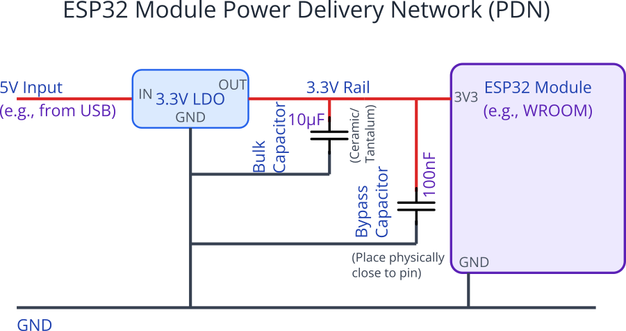
- Voltage: All ESP32 variants operate at a nominal 3.3V. It is critical that your voltage regulator can supply this voltage cleanly and with minimal dropout, even under heavy load.
- Current: Check the datasheet for the specific variant’s peak current draw. A dual-core ESP32-S3 under heavy load can draw over 500mA in short bursts. Your 3.3V regulator should be rated accordingly (e.g., 800mA or 1A to be safe). A cost-optimized ESP32-C3 will have a lower peak draw, but it is still significant.
- Decoupling Capacitors: These are non-negotiable. Decoupling capacitors act as tiny, local reservoirs of charge, supplying the chip during sudden current spikes that the main regulator can’t respond to quickly enough.
- Bulk Capacitor: Place a larger capacitor (typically 10µF, ceramic or tantalum) near the module’s 3.3V power input pin. This provides bulk energy storage.
- Bypass Capacitors: Place smaller capacitors (typically 100nF or 0.1µF, ceramic) as close as physically possible to every power pin on the module.
- Rule of Thumb: If you are unsure, add more decoupling. It’s a cheap insurance policy against intermittent crashes and bizarre behavior. The specific values and placement are always detailed in the official Hardware Design Guidelines.
Pillar 3: RF Layout and Antenna Design
The radio is the core feature of the ESP32. A poor RF layout will result in poor connectivity, reduced range, and failed transmissions.
- Modules with Onboard PCB Antenna: Most common modules (e.g., ESP32-WROOM-32E, ESP32-C3-MINI-1) have an integrated meandered inverted-F antenna (MIFA) etched directly onto the module’s PCB.
- Keep-Out Zone: This is the most critical rule. The antenna portion of the module must not have any copper (traces, ground planes, component pads) on any layer of your main PCB underneath or around it. The datasheet specifies the exact dimensions of this keep-out area. Violating this rule will detune the antenna and cripple its performance.
- Placement: For best performance, place the module at the corner or edge of your PCB, so the antenna radiates into free space, not into the rest of your circuit. Avoid enclosing the device in a metal case, which will form a Faraday cage and block all RF signals.
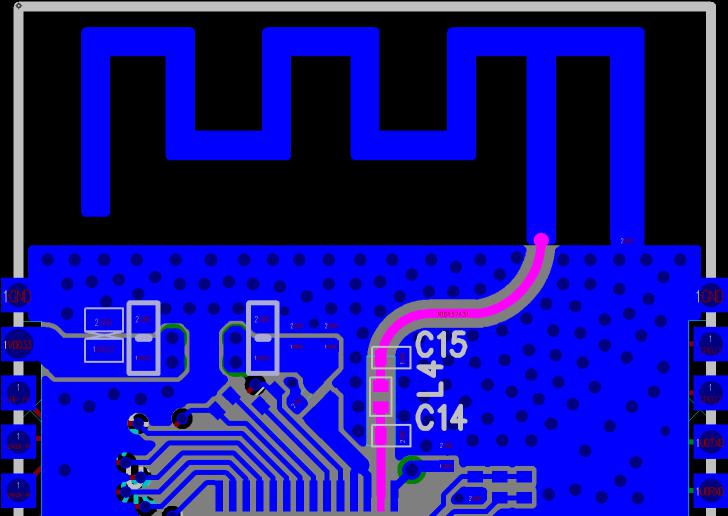
- Modules with External Antenna Connector (U.FL): Some modules come with a small U.FL connector for an external antenna. This is useful when the device must be in a metal enclosure, allowing the antenna to be mounted externally. The same keep-out rules apply around the U.FL connector and its feedline.
- Variant-Specific RF:
- Wi-Fi & Bluetooth: Share the same 2.4 GHz antenna.
- ESP32-C6 / ESP32-H2: These chips have two radios: one for 2.4 GHz Wi-Fi/BLE and a second for the 802.15.4 (Thread/Zigbee) protocol, which also operates at 2.4 GHz. On modules, these are typically handled by an internal RF switch and share a single antenna. The complexity is managed for you on the module.
Pillar 4: Strapping Pins and Boot Modes
Strapping pins are special GPIOs that are read by the ESP32 during power-on or reset. Their voltage level (HIGH or LOW) at that moment determines fundamental chip settings like the boot mode and the operating voltage for the internal flash memory.
- What they control:
- Boot Mode: The most important one is
GPIO0. IfGPIO0is pulled LOW during boot, the chip enters “Download Mode,” waiting for new firmware to be flashed via the UART. If it’s HIGH (or floating), it enters the normal “Run Mode,” executing the code from flash. - Flash Voltage (VDD_SDIO): Pins like
GPIO45(on S3) orMTDO(GPIO15on ESP32) can select the voltage for the flash chip.
- Boot Mode: The most important one is
- Variant Differences: The strapping pins are different for each ESP32 variant. You must consult the datasheet for the specific chip you are using. An incorrect pull-up or pull-down resistor on a strapping pin will prevent your board from booting correctly.
- Implementation: These pins are typically controlled by the USB-to-UART chip (like a CP2102 or CH340) in a typical development board circuit to automatically toggle between Run and Download modes. For a production device, you will use pull-up or pull-down resistors to permanently set the desired state (e.g., a 10kΩ pull-up on
GPIO0for Run Mode).
flowchart TD
    subgraph ESP32 Power-On/Reset Sequence

    A(Power On / Reset) --> B{Read Strapping Pins};

    B --> C{GPIO0 Level?};

    C -- "LOW (Pulled to GND)" --> D[Enter Download Mode];
    C -- "HIGH (Pulled to 3.3V or Floating)" --> E[Enter Run Mode];

    D --> F[Wait for Firmware via UART];
    F --> G{Flash Successful?};
    G -- Yes --> H(Reboot);
    G -- No --> F;

    E --> I[Load Program from Flash];
    I --> J[Execute Application Code];

    end

    %% Styling
    classDef primary fill:#EDE9FE,stroke:#5B21B6,stroke-width:2px,color:#5B21B6;
    classDef decision fill:#FEF3C7,stroke:#D97706,stroke-width:1px,color:#92400E;
    classDef process fill:#DBEAFE,stroke:#2563EB,stroke-width:1px,color:#1E40AF;
    classDef success fill:#D1FAE5,stroke:#059669,stroke-width:2px,color:#065F46;
    classDef fail fill:#FEE2E2,stroke:#DC2626,stroke-width:1px,color:#991B1B;

    class A,H primary;
    class B,C,G decision;
    class D,E,F,I process;
    class J success;
Example: Strapping Pins for ESP32-S3 vs ESP32-C3
| Function | ESP32 (Classic) | ESP32-S3 | ESP32-C3 |
|---|---|---|---|
| Boot Mode Select | GPIO0 | GPIO0 | GPIO9 |
| Required State for Run Mode | Pulled HIGH or Floating | Pulled HIGH or Floating | Pulled HIGH or Floating |
| Required State for Download Mode | Pulled LOW | Pulled LOW | Pulled LOW |
| Flash Voltage (VDD_SDIO) | MTDI (GPIO12) 0=3.3V, 1=1.8V |
GPIO45 0=3.3V, 1=1.8V |
Not a strapping pin. Controlled internally or via eFuse. |
| JTAG / Debugging | MTDO (GPIO15) Disables debug log on UART0 if pulled HIGH. |
GPIO46 Selects ROM messages output. |
GPIO8 Selects ROM messages output. |
| Master Enable | EN / CHIP_PU | EN / CHIP_PU | EN / CHIP_PU |
Tip: The
EN(Enable) orCHIP_PUpin is the master switch. It must be pulled HIGH for the chip to run. A simple RC circuit (10kΩ pull-up, 0.1µF to ground) is often recommended on the EN pin to ensure a clean startup sequence.
Pillar 5: Pin-Outs and Peripherals
While the ESP-IDF provides a consistent software API, the physical pins that peripherals are connected to vary significantly.
- GPIO Count: High-performance chips have more pins.
- ESP32/ESP32-S3: Offer a large number of GPIOs (up to 45 on the S3), making them suitable for complex applications with many sensors and actuators.
- ESP32-C3/ESP32-C6: Have a much lower GPIO count (around 22) as part of their cost-optimized design.
- Specialized Peripherals:
- USB OTG: The ESP32-S2 and ESP32-S3 feature a native USB interface on
GPIO19(D-) andGPIO20(D+). This requires careful routing on the PCB (as a 90Ω differential pair) and eliminates the need for an external USB-to-UART converter chip, potentially reducing BOM cost. - ADC/DAC: The specific GPIOs that can be used for Analog-to-Digital Conversion (ADC) or Digital-to-Analog Conversion (DAC) differ. Some ADCs are more sensitive or have better linearity. The S2/S3/C3/C6 have improved ADC performance over the original ESP32.
- PSRAM: On modules like the ESP32-WROVER (original ESP32) or ESP32-S3-WROOM modules with octal-SPI PSRAM, the pins for the PSRAM are internally routed. You don’t have to worry about them, but you also lose those GPIOs for general-purpose use.
- USB OTG: The ESP32-S2 and ESP32-S3 feature a native USB interface on
- The Golden Rule: Always have the correct module datasheet open when designing your PCB. Never assume a pin function is the same as on another variant you’ve used before.
| Feature / Peripheral | ESP32 (Classic) | ESP32-S3 | ESP32-C3 | ESP32-C6 |
|---|---|---|---|---|
| CPU Core(s) | Dual-Core LX6 | Dual-Core LX7 | Single-Core RISC-V | Single-Core RISC-V |
| Max GPIOs (approx.) | ~34 | ~45 | ~22 | ~30 |
| Native USB OTG | ✗ No | ✓ Yes (GPIO19/20) | ✗ No (Serial/JTAG only) | ✗ No (Serial/JTAG only) |
| Wi-Fi | 2.4 GHz Wi-Fi 4 | 2.4 GHz Wi-Fi 4 | 2.4 GHz Wi-Fi 4 | 2.4 GHz Wi-Fi 6 |
| Bluetooth | BLE 4.2 & Classic | BLE 5.0 | BLE 5.0 | BLE 5.3 |
| 802.15.4 (Thread/Zigbee) | ✗ No | ✗ No | ✗ No | ✓ Yes |
| PSRAM Support | Quad SPI | Octal SPI | ✗ No | Quad SPI |
| ADC Channels | Up to 18 | Up to 20 | Up to 6 | Up to 7 |
| DAC Channels | 2 (8-bit) | ✗ No | ✗ No | ✗ No |
Common Mistakes & Troubleshooting Tips
| Mistake / Issue | Symptom(s) | Troubleshooting / Solution |
|---|---|---|
| Inadequate Power Decoupling | – Board randomly crashes or reboots, especially under load (e.g., Wi-Fi scanning). – “Brownout detector was triggered” error in logs. – Unexplained, glitchy behavior. |
1. Add a 10µF bulk capacitor near the module’s 3.3V input. 2. Add a 100nF (0.1µF) bypass capacitor as close as physically possible to EVERY 3.3V power pin on the module. 3. Ensure power traces are wide enough for the current. |
| Incorrect Strapping of GPIO0 | – Board never runs application code. – Immediately enters Download Mode on every boot. – Works only when a programmer (like an FTDI chip) is holding the pin HIGH. |
Add a 10kΩ pull-up resistor from GPIO0 (or the equivalent boot pin for your variant, e.g., GPIO9 on C3) to 3.3V. This ensures the chip boots into “Run Mode” by default. |
| EN / CHIP_PU Pin Floating | – The board is completely unresponsive. – No serial output, no power consumption. – The chip is never enabled. |
The EN (Enable) pin MUST be pulled HIGH. Add a 10kΩ pull-up resistor from the EN pin to 3.3V. For extra stability, also add a 0.1µF capacitor from EN to GND. |
| Antenna Keep-Out Zone Violation | – Extremely poor Wi-Fi/Bluetooth range. – Device can only connect when inches from the access point. – Unstable connection, frequent disconnects. |
The area under and around the module’s PCB antenna must be completely clear of copper (ground planes, traces, components) on ALL layers of your main PCB. Re-spin the board with a proper keep-out zone as specified in the datasheet. |
| Incorrect Flash Voltage Strapping | – Board fails to boot. – Gibberish or “invalid header” errors on the serial monitor. – The ROM bootloader cannot read the flash chip. |
Check the strapping pin for VDD_SDIO (e.g., GPIO12 on ESP32, GPIO45 on S3). Ensure its pull-up/pull-down state matches the voltage required by your specific module (usually 3.3V). Refer to the module datasheet. |
| Swapped UART TX/RX Lines | – Flashing fails with timeout errors. – You see boot messages from the ESP32, but cannot send any commands to it. |
Double-check your connections. The module’s TXD0 pin should go to the programmer’s RX pin. The module’s RXD0 pin should go to the programmer’s TX pin. |
Exercises
- Datasheet Detective: Download the official datasheet for an ESP32-C6-MINI-1 module from the Espressif website. Identify the following:
- The pin number for the
ENpin. - The pin number for the boot mode strapping pin (equivalent to
GPIO0). - The dimensions of the antenna keep-out area.
- The recommended value for the bulk decoupling capacitor at the power input.
- The pin number for the
- Layout Review Challenge: A colleague sends you the following description of their PCB layout for an ESP32-S3-WROOM-1 module. Identify at least three major hardware design flaws.”I placed the ESP32-S3 module right in the center of the board to make routing easier. The 3.3V power comes from a 150mA LDO. I put a single 22µF capacitor next to the LDO. To save space, I ran the USB D+/D- traces right next to the 2.4GHz antenna trace from an external antenna connector. The board is in a sealed aluminum case for protection.”
- Minimal Circuit Design: You need to design a minimal “breakout board” for an ESP32-C3-WROOM-02 module. Your goal is to get it to boot and be programmable over UART. List the essential external components (resistors, capacitors) and state their purpose and connection points (e.g., “10kΩ pull-up resistor on pin X”). You can ignore the USB-to-UART chip itself and assume its DTR/RTS lines are available to control boot mode.
Summary
- Use Modules: For almost all projects, using pre-certified modules is the best approach to simplify design and avoid regulatory hurdles.
- Power is Paramount: A stable 3.3V supply with sufficient current capacity and meticulous decoupling is non-negotiable.
- Respect the RF Keep-Out: The single most common failure point in custom hardware is a poorly designed antenna layout. Keep the antenna area clear!
- Strapping Pins Dictate Boot: Incorrect pull-up/pull-down resistors on strapping pins will prevent your board from starting correctly.
- Datasheets are Your Source of Truth: Never assume pin-outs or hardware requirements are the same between variants. Always work from the official datasheet and Hardware Design Guidelines for your specific module.
- Differences are Features: The variations in peripherals like native USB, GPIO count, and radio capabilities are what allow you to pick the perfect, most cost-effective chip for your specific application.
Further Reading
- Espressif Hardware Design Guidelines: This is the most important document for any ESP32 hardware designer.
- ESP32 Module Reference Designs: The schematics and PCB layouts for Espressif’s own development kits are an invaluable resource.
- ESP32-S3-WROOM-1 & 1U Datasheet: An example of a modern module datasheet containing footprint, schematic, and peripheral information.